Description
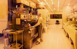
The course provides an in-depth understanding of top-down device fabrication. Focus is the unit processes typically used in micro & nanofabrication of devices. Both concepts and practical aspects are covered. Topics include crystal growth, doping, chemical vapor deposition, physical vapor deposition, photolithography, wet etching, dry etching, and packaging. The course is accessible to students from diverse backgrounds, such as materials, physics, chemistry, mechanical engineering, and electrical engineering.The course will be a derivative of NE203: Advanced Micro & Nano Fabrication Technology & Processes. Students from various departments outside CeNSE, e.g. Physics, Chemistry, ECE, DESE, IAP, routinely take the course.
ABOUT THE INSTRUCTOR
Prof.Shankar Kumar Selvaraja obtained B.E. Electronics and Communication Engineering from Dr. MCET, Pollachi, Bharathiar University, M.E. Optical Communication from College of Engineering, Anna University, Chennai, M. S. Microelectronics and Microsystems from University of Twente, The Netherlands and Ph.D. in Photonics Engineering from Ghent University, Belgium in 2011. His doctoral thesis was carried out at imec (inter-university microelectronics center), Leuven, Belgium on wafer-scale fabrication technology for Silicon photonic integrated circuits. He was supported by Dehouse doctoral grant and scientific leadership training award to conduct his doctoral work. Between 2011 and 2014, he worked at imec, Belgium developing next-generation microprocessor for high-speed computing using Silicon photonic integrated circuits. He has spent a decade in the area of silicon photonic developing state-of-the-art process and device technology for Silicon Complementary-Metal-Oxide-Semiconductor (CMOS) compatible photonic integrated circuit for high-speed optical interconnect. Dr.Shankar Kumar Selvaraja joined Centre for Nano Science and Engineering at Indian Institute of Science (IISc) in 2014 as an Assistant Professor, where he is heading the Photonics Research Laboratory. He is currently deputy chairman of the National Nanofabrication Center at IISc. He was awarded Early Career Research Award by Department of Science and Technology-Science and Engineering Research Board (DST-SERB), Government of Indian. In 2014, he was awarded Sir Visvesvaraya Young Faculty Research Fellowship by Ministry of Electronics and Information Technology (MeitY), Government of India. He is a senior member of IEEE (Institute of Electrical and Electronics Engineers), Member of OSA (Optical Society of America) and SPIE. His current area of research includes high-speed Si photonics, Silicon Nitride photonics circuits, microwave photonics, and on-chip mic-IR sensing technology.

Prof.Sushobhan has worked in the field of semiconductor device fabrication technology for more than 10 years, specializing on photovoltaics. His PhD thesis was on organic/Si heterojunction silicon solar cells. He then worked as a post-doctoral research associate in the Princeton Institute of Science and Technology of Materials (PRISM), where he worked on oxide/Si heterojunction solar cells. Since 2014, he has been working an assistant professor in the Indian Institute of Science at the Centre for Nano Science and Engineering (CeNSE), Indian Institute of Science (IISc). In 2014, he was awarded Sir Visvesvaraya Young Faculty Research Fellowship by Ministry of Electronics and Information Technology (MeitY), Government of India. In 2018 he was awarded the Young Engineer Award by the Indian National Academy of Engineers (INAE). He is a young associate of the INAE, member of IEEE (Institute of Electrical and Electronics Engineers), and member of MRS. Sushobhans current research interests are thin-film photovoltaics, heterojunction solar cells, and metal-oxide electronics. He has authored over 30 research papers and holds a Taiwanese patent (US and European patent applications pending).Sushobhan is a member of the Administration Committee of the National Nanofabrication Facility at CeNSE. He is also a member of the Institute Safety Committee and Safety warden for CeNSE


Reviews
There are no reviews yet.